Choose timezone
Your profile timezone:
X-ray waveguides have attracted a great deal of attention because of their application in x-ray optics for producing intense coherent nanobeams. However, a 1D planar x-ray waveguide structure also provides a powerful tool to study the properties of the guiding layer itself. Multiple reflections of the x-rays from the walls of the waveguide result in a significant redistribution of x-ray intensity across the depth of thee guiding layer. Resonance modes of such a planar waveguide can be excited for the angle of incidence of x-rays satisfying the condition 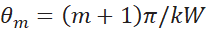 , where k is the propagation vector of the x-rays and W is the width of the cavity, and m is an integer. Such structures have been exploited by us in a variety of ways to study the guiding layer itself.
i) Firstly, the positions of the waveguide modes depend upon the thickness and density of the guiding layer alone. Thus, any changes in these parameters due to factors like interdiffusion or defect creation can be monitored precisely. ii) By selecting the angle of incidence corresponding to TE0 or TE1 mode of the waveguide, any x-ray based measurement can be made sensitive either to the center of the guiding layer or to its interfaces, respectively. Of particular interest are the structures like HM/CoFeB/HM (HM=heavy metal), which exhibit a variety of phenomena like spin orbit torque, interfacial DM interaction, perpendicular magnetic anisotropy. All these phenomena depend sensitively on the structure of the interfacial region, which can be explored selectively by tuning the angle of incidence of x-rays. We have demonstrated that almost all x-ray based techniques like XRD, XAFS, HAXPES, NRS can be made depth-selective in this manner. Selected results on W/CoFeB/W and Mo/CoFeB/Mo multilayers will be presented. iii) Furthermore, the x-ray waveguide structures can be used for depth profiling of a marker layer inside the guiding layer with sub-nanometer accuracy. This is achieved by placing the marker layer asymmetrically between the antinodes of TE1 and TE2 modes and measuring the angle dependent fluorescence from the marker layer. The technique has been used to measure Kirkendall shift in nanocrystalline films. Results on Kirkendall shift in nanocrystalline iron films will be presented, which show that microstructural variation can lead to a net mass transfer even within a chemically homogeneous film.